The material in this section shows how we built the Twist-Shift system for VHF using commonly available (and cheap) surplus land mobile VHF transceivers modified to operate on the 2-meter ham band. The radios we used were the 100-watt Motorola SyntorX model. The radios were additionally modified for the Twist-Shift experiments as described below. This section also describes the auxiliary circuitry needed to implement the system and the test setup for the experiments we ran to prove that the concept works and to quantify just how well it works.
This page describes the VHF Twist-Shift Keying setup using the SyntorX radios. The material is presented, not as a hard and fast specification of equipment and circuitry, but as an example of how Twist-Shift can be implemented.
As presented in Discription/Rationale, all of the basic components for Twist-Shift transmission and reception must be provided. These are:
-
An orthogonal antenna at the transmit end of the transmission path.
-
A method for driving the transmitting antenna elements 'in quadrature', that is, with two precisely synchronized sources of RF energy offset in phase by 90 degrees.
-
A method for reversing the phase of one of the RF sources. (The phase reversals carry the data.)
-
An orthogonal antenna at the receive end.
-
A dual synchronized receiving system that provides separate paths for the orthogonal signals picked off from the receiving antenna. Synchronization requires that injection sources for all mixers in the system be driven from a common source. The receiving system must also be "normalized", that is, the two signal paths must be brought back into zero-degree phase synchronicity.
-
Some type of multiplier (detector) to recover the phase reversals and thus the transmitted data.
-
A filter after the detector.
ANTENNAS
The cross-polarized antennas we used for feasability testing are shown here. They consist simply of two j-pole type elements cut for a resonant frequency of 146 MHz mounted orthogonally. The transmit antenna was suspended from the rafters of an outbuilding on my property 50 meters distant from my shop where an identical receive antenna was likewise suspended from the ceiling. Calculated path loss from the transmit end to the receive end was 50 dB. Later, the j-pole elements were incorporated into a cross-polarized yagi design. Two of these antennas were used to check the system at 1 mile range.
[We used home-constructed antennas for our experiments. The Hy-Gain model 216SAT would appear to be an equivalent, commercially available alternative to our antennas.]
TEST TRANSMITTER
Our test setup is shown in Figure 1.
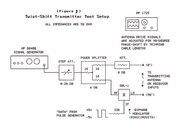
The output from the signal generator is reduced in level by the adjustable attenuator and split into two identical feeds at 0 dBm or less. Modulation takes place in the Minicircuits SBL-1 driven by a bipolar data signal from a pulse generator. The SBL-1 serves to either 1) reverse the phase of the RF drive signal through the device, or 2) NOT reverse the drive signal (pass it through un-affected). The state of the data signal input, introduced into the IF port, determines whether the RF signal is reversed or not. In other words the SBL-1 is a biphase modulator. The pad shown in the leg of the circuit without the SBL-1 is used to balance the drive levels so as to produce a more perfectly circularized radiated signal. Normally the setting of that attenuator is zero. The antenna drive signals were adjusted for perfect quadrature by trimming the antenna drive cable lengths using an HP 1725, 250 MHz dual-channel oscilloscope. (A good 100 MHz scope will work also.)
High-Power Twist-Shift Transmitter
We used a Motorola SyntorX transmitter, modified for operation on 146 MHz, as the signal source for our high-power tests. Modification of the Syntor X radio for 2-meter operation is beyond the scope of this article, but it's not terribly hard to do. The modification consists mainly of replacing the EPROM in the radio's synthesizer with one programmed for 2-meter frequencies, and maybe some retuning. Here's some mod info John West put together. [John can also provide stock or modified-for-2-meter SyntorXs and programmed EPROMs. Inquire .] Typing "Syntor 2-meter modification" into a search engine will also yield a wealth of information.
Figures 2 shows an example of how a high-power (2 x 100-watt) Twist-Shift modulated transmitting system can be constructed using two Syntor X radios.
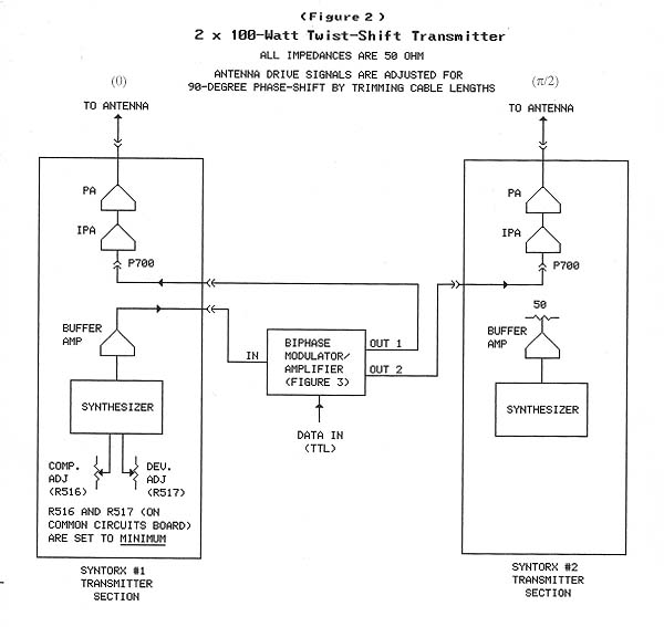
Figure 3 shows the schematic for the biphase modulator shown in the figure above.
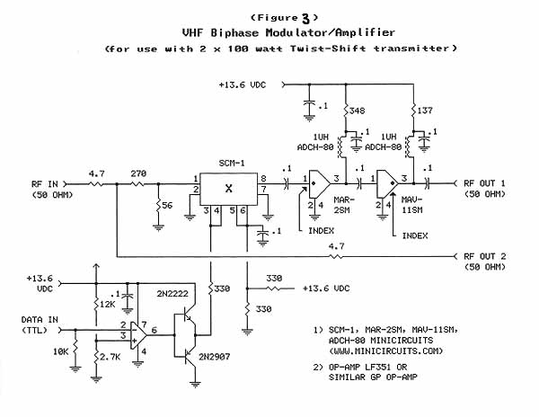
The circuit consists of a power splitter/attenuator that reduces the drive level to the SCM-1 balanced mixer by about 25 dB (the SCM-1 is electrically equivalent to the SBL-1). The phase modulated output from the mixer is then amplified about 25 dB and delivered to the RF OUT 1 jack. A non-modulated output is delivered to the RF OUT 2 jack.
Figure 4 shows an alternate biphase modulator.
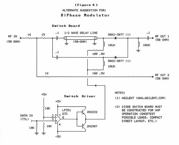
In this version the signal power is first divided, then passed through a 180-degree delay line and presented to a diode switch. The conduction state of the switching diodes (driven by the data input) determines whether the signal delivered to the RF OUT 1 jack is phase-shifted or not. A non-modulated output is delivered to the RF OUT 2 jack. [Note: The output power from this circuit is about about 5 dB lower than the +15 dBm output power from the biphase modulator/amplifier shown in Figure 3. This (+10 dBm) is still considerably greater than what is required to drive the Syntor X transmitters to full output power (typically 150 watts when powered from a 14.4 VDC source).]
[Transmitter Modification Details.]
RECEIVING SYSTEM
The receiving system is more complicated and requires two more radios. [With a little ingenuity, the transmitter and receiver sections from two radios probably could be combined into a half-duplex station.] The two SyntorX receivers are synchronized to a common reference oscillator, as shown in Figure 5.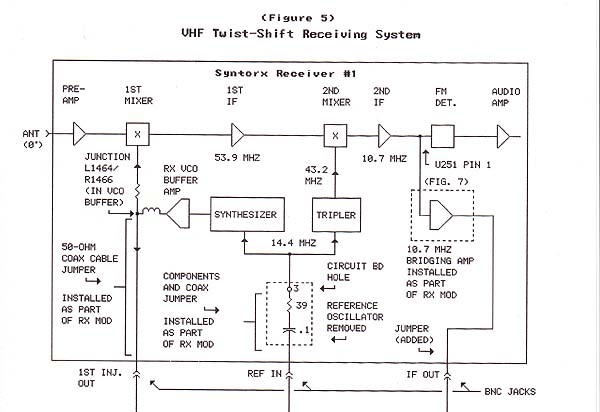
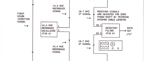
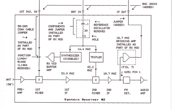
The external reference oscillator drives the first mixer injection synthesizer and the second mixer injection tripler in both radios. [Note that the receiver synthesizer and the transmitter synthesizer in each radio are one in the same. The synthesizers are reconfigured when the radios are in the transmit mode.] The synthesizer in the slave radio is disabled and the output from the synthesizer in the master radio is used to drive the first mixer in BOTH radios. [It was found that the two synthesizers could not be synchronized well enough to be used at the same time to drive their respective mixers. They exibited excessive phase wander.] Thus, since all of the mixers in the system are driven from a common source, the two signal paths operate coherently, which is to say, (after normalization) the IF outputs signals from the two receivers maintain the same phase relationship as the input signals.
Here's a photo of the receiver setup.
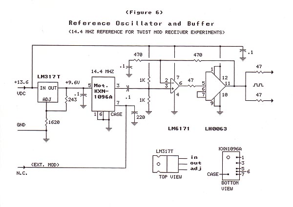
The external 14.4 MHz reference oscillator is constructed from one of the reference oscillators removed during modification of the radios. The schematic is shown in Figure 6.
Here's a photo of the constructed reference oscillator.
The circuit schematic for the bridging amplifiers is shown in Figure 7.
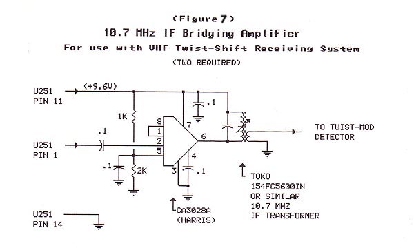
Each bridging amplifier is constructed on a small (1.2" x .8") perfboard (photo). The transformer is tuned for maximum output with a 10.7 MHz test signal input. When tuned, the amplifier has a gain of about 1000 measured at pin 6 of the CA3028A.
[Receiver Modification Details.]
DETECTOR/FILTER
The schematic for the detector/filter is shown in Figure 8.
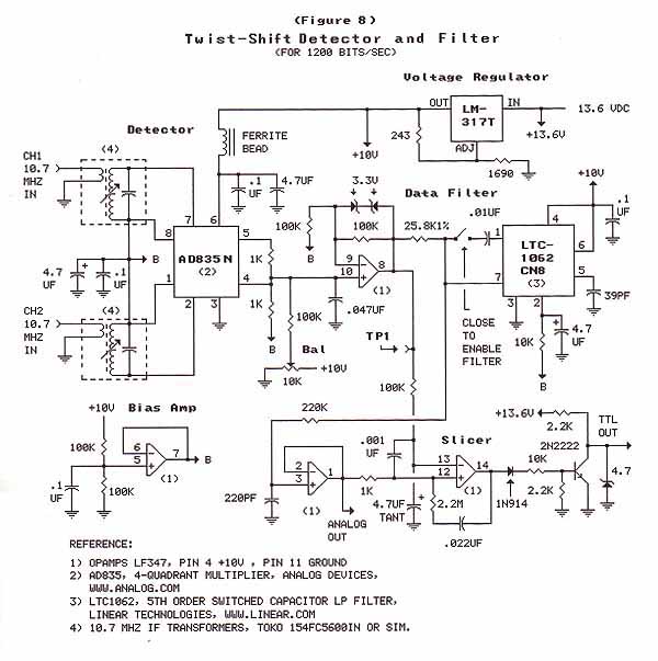
The heart of the circuit is the AD835 multiplier chip which serves as a phase comparator. The chip outputs a signal that is proportional to the instantaneous product of the input signals (up to the chip's bandwidth, set by capacitor C3) . As outlined above, the 10.7 MHz input signals from the receiving system will have been "normalized" as part of the optimization procedure. Thus, depending on the 'twist-state' of the received signal (CW or CCW), the input signals will assume one of two states: 1) in-phase (0-degree phase offset), or 2) out-of-phase (180-degree offset). This will cause the output of the detector (pin 5) to assume one of two states: 1) above the bias voltage (B), or 2) below the bias voltage. This signal constititutes the raw data output of the system. The raw data signal is amplified, filtered by the LTC1064 switched-capacitor low-pass filter and presented to the slicer where it is compared with a filtered DC average from the detector and a 1/0 decision is made. The output from the slicer is converted to a TTL-level (5 volt) output which can be used to drive a computer or other terminal equipment.
Here's a photo of the as-built detector filter.
DETECTOR ADJUSTMENT NOTES
- A DC voltmeter is connected between pin 7 of the bias amplifier and TP1. With no signal input, the BAL control is adjusted for zero volts.
- [This adjustment requires the phase-normalized transmitting test setup shown in Figure 1 be used as the signal source. The receiver, likewise, should be fully normalized before making the adjustment.] A scope is connected to TP1 and the 10.7 MHz IF transformers are adjusted for maximum amplitude of the recovered data signal. The 10.7 MHz transformers in the bridging amplifiers should also be adjusted at this time.
The circuit is very forgiving of less-than-perfect input signals. As mentioned, large deviations from perfect circularity, in both phase and amplitude, are well handled. Perfection, however, should be strived for in adjusting system phasing. A 100 MHz or greater, dual-channel oscilloscope, will be indispensable in this effort.