Frequency Controller
Add-On Circuit Disciplines Ovenized Crystal Oscillator
Oscillator frequency maintained accurate to better than 10 parts/1011 long-term.
See system limits below.
This is the third article in a series. Read first:
WWVB-Based Precision Frequency Comparator
and
Computer-Interfaced Version.
|
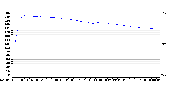
This circuit is an adjunct to the computer-interfaced version of the basic WWVB-precision frequency comparator. It takes the 8-line digital parallel output from the comparator's counter/accumulator, converts the data to an analog voltage and presents it back to the frequency control pin of the ovenized oscillator (OCXO) to "discipline" its frequency. The basic D/A circuit was lifted from the data sheet for the AD7524 digital to analog converter chip. A block diagram of the complete system is shown in Figure 5 below. Figure 6 shows the schematic for the frequency controller. (Figure 5) Block Diagram, Frequency Controller Added to WWVB Comparator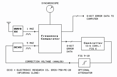 (Figure 6) Controller Schematic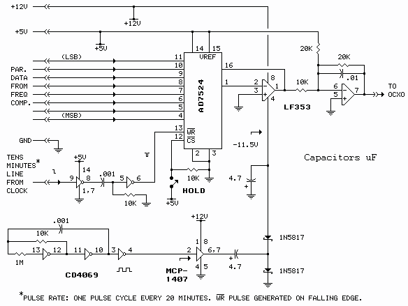 The circuit consists of the AD7524 D/A converter, a couple of general purpose JFET op amps, input conditioning for the sample signal, and an oscillator/charge pump that develops the negative power supply rail for the op amps. Digital error data in the form of an 8-bit binary word from the frequency comparator is clocked into the D/A converter 3 times per hour under control of the "sample" input line. The sample signal comes from the BCD "10s minutes" line of a digital clock (this particular digital clock is part of the WWVB receiver). This line goes high on odd numbered multiples of 10 minutes and low on even-numbered multiples. In other words, the line goes high at 10, 30 and 50 minutes past the hour and low at 0, 20 and 40 minutes past the hour. The controller input logic selects the high-to-low transition of the sample clock and delivers a short (10µS) negative-going pulse to the D/A converter, at which time the data is clocked into the internal latches of the AD7524. The data held in the latches controls the voltage output from the D/A converter until the next sample pulse is received 20 minutes later. In other words, the output voltage can change 3 times per hour, at 0, 20 and 40 minutes past the hour. Almost any clock interval could have been used as the sample clock source, but using this particular interval avoids the 10 minutes past/15 minutes past window in which WWVB is shifting its carrier phase. The voltage output from the controller, and thus the frequency of the ovenized oscillator, remains unperturbed during that time period. [Update: The ±45° phase shift at 10/15 past the hour will be discontinued in 2012.] The voltage output from the D/A converter appears on pin 7 of the op amp pair. The output voltage depends on three factors: the reference voltage on Vref input pin 15 (+5 volts), the gain of the second op amp (x2), and the binary input word. The voltage on the output pin ranges from a high of +5 volts with an input word at binary 11111111 (decimal 255), to a low of -5 volts with the input word at binary 00000000 (decimal 0), a range of 10 volts. Each one-count change in the input word produces a change of 10/256 volts (.039 V) in the output. The relationship of the input word to the output voltage is direct: a larger-value input word produces a more-positive output voltage. This satisfies the requirement for the ERC OCXO that a more-positive input voltage on the control pin produces a lower output frequency. In other words, the comparator and controller are connected so as to produce negative frequency feedback - increasing frequency produces a higher controller output voltage, which forces the OCXO to operate at a lower frequency. For OCXOs that require a more-negative input voltage to produce a lower frequency, the circuit can be changed, as shown in Figure 7. (Figure 7) Negative Voltage ReferenceTo change the input word/output voltage relationship to inverse (larger input word produces a more-negative output voltage), add the 5v zener diode and 6.8k resistor as shown. There should be no connection from pin 15 to +5V. 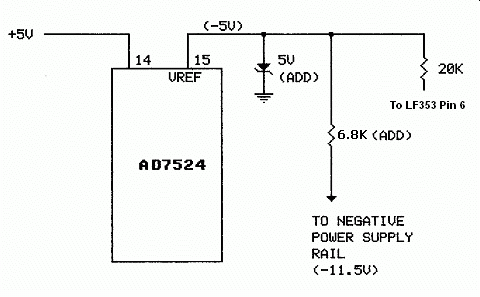 The analog output from the controller is connected to the ovenized crystal oscillator as shown in Figure 8. (Figure 8) OCXO Connection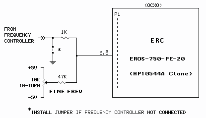 For the ERC EROS-750-PE-20 (and HP10544A) the connection is made to pin 6 and 6 of P1 on the oscillator's edge connector (Fig 8). The oscillator's free-running frequency must have been pre-adjusted to place it within the controller's lock range. This is accomplished using the synchroscope display described in the first article of this series, WWVB-Based Precision Frequency Comparator, or by other means. The optional gain control (Fig 9) can be used to lower the gain of the control loop, if necessary, to minimize "hunting" - constant meandering back and forth from one frequency extreme to another. Turn the gain up until hunting starts; lower the gain until hunting just stops. [The gain control was initially helpful with the ERC oscillator but, after several years of oscillator aging, has become lately unnecessary, ie, the gain control is now set to maximum (minimum attenuation).] Keep in mind that reducing the gain of the control loop will lower the system's lock range and may affect long-term stability, see below. (Figure 9) Optional Gain Control 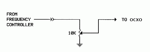 Another approach to gain control is the step attenuator shown in Figure 10. (Figure 10) Stepped Gain Control 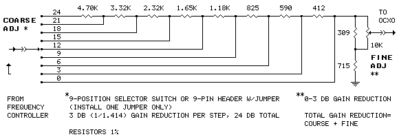 Each step produces a gain reduction of about 0.7 (3dB). The selector can be implemented with a switch or pin header and jumper. Total gain reduction is equal to the step setting plus the setting of the FINE control. PhotosThe controller circuitry is contained on this board which "piggybacks" on the main board in the comparator. 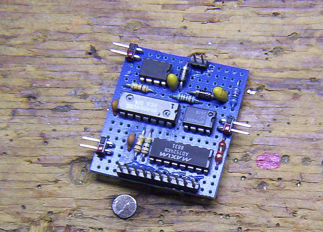 The ERC OCXO is the silver/black square thing on the upper right. The meter monitors the controller output voltage. The WWVB receiver is at the bottom. The comparator/controller is above the WWVB receiver. 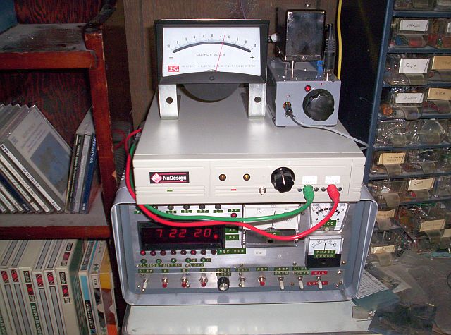 System Limits: PlesiochronicityNote that, due to the phase slip dependent/stepped nature of voltage output from the controller, the described system is plesiochronous. In other words, the output frequency will be very close to dead on compared to WWVB and the atomic standard that drives it over a long time frame (24 hours or more) but will not be perfectly phase synchronous, that is, the controlled oscillator will exibit some degree of phase wander. The degree of asynchronicity is dependent on the native stability of the OCXO and the setting of the optional loop gain control (Fig. 9 or 10). The setting of the gain control affects long-term and short-term stability in opposite directions - higher gain settings improve long-term stability while lower gain settings improve short-term stability. The sweet-spot setting is the point where hunting just stops (see gain control above). Shown below are a couple of snapshots showing the performance of the WWVB comparator/controller driving the ERC EROS-750-PE-20 OCXO over a 31-day period. The graphs were made with the WWVB-Based Precision Frequency Comparator, Computer-Interfaced Version. The large perturbation near the beginning of the period is due to a manual/mechanical readjustment of the ERC OCXO. As you can see, after the system stabilized on day 3, the controller struggles a bit over the 12-hr intervals to meet that 10 parts/1011 claim (first graph). However, averaged over the 28-day interval (second graph), the goal is met: Frequency - 31-Day Graph
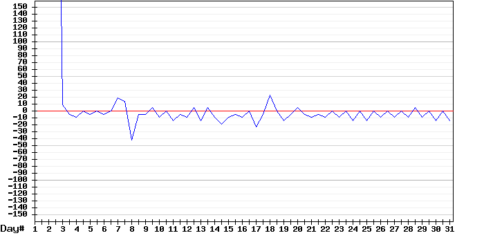 12-Hour Average Phase Slip Count (N) and Correction Voltage - 31-Day Graph
(How would a genuine HP10544A perform? A 10544A is currently being tested [here].) And the point of this exercise?It demonstrates that the accuracy of this particular source can at least be improved by a factor of 100 (compared to the manual adjustment approach shown in the first WWVB/Comparator article in this series) by simply "looping back" the accumulated slip data (after D/A conversion) to directly control its frequency. A more sophisticated algorithm contained in a microcontroller might do better, say by analyzing the long-term drift and applying preemptive correction. But then again it might not. The native stability of the OCXO, along with the WWVB receiver and propagation issues noted in that first article may be limiting factors too great to overcome. Some PLL (phase locked-loop) math probably would be helpful. Characterizing the various components (phase comparator, loop filter) and parameters (loop gain, damping) might be challenging. top↑ |
Addendum: Hewlett Packard 10544A Tested with the ControllerOK, I finally got around to a 31-day run with a 10544A; the results are shown below:
Frequency - 31-Day Graph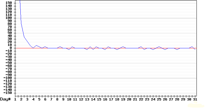 12-Hour Average Phase Slip Count (N) and Correction Voltage - 31-Day Graph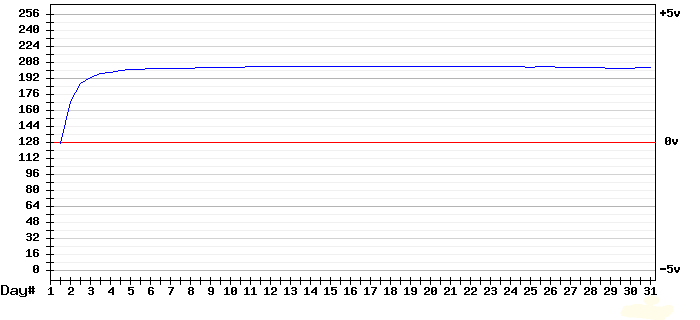
The 10544A clearly outperforms the ERC unit above, especially regarding long-term stability (second image). The calculation is: Free Run OptionAfter seeing this result, I added a free-run option to the controller. This is a defeat switch that inhibits the D/A converter (AD7524) update pulse from the clock, allowing the oscillator to free run on its most recently-loaded correction voltage. The free-run switch (HOLD) is shown Figure 6. Schematics produced with DCCAD. |
